

Via-In-Pad
Via-in-pad technology has revolutionized the way printed circuit boards (PCBs) are designed, particularly in applications requiring high-density interconnects (HDI) and compact layouts. This technique involves placing vias directly within the surface mount pads of components, offering a practical solution to meet the ever-growing demand for smaller, faster, and more reliable electronic devices. By combining space efficiency with enhanced electrical and thermal performance, via-in-pad has become an indispensable feature of modern PCB designs.
The most immediate advantage of via-in-pad is its ability to conserve board space. As electronic devices shrink in size, engineers are tasked with designing intricate PCBs that accommodate numerous components in a limited area. Traditional via placement often requires additional routing space, making it difficult to achieve the desired compactness. Via-in-pad resolves this issue by embedding vias within the component pads themselves, effectively merging two critical functions into a single footprint. This approach simplifies routing, reduces congestion, and allows for more compact and efficient designs.
From an electrical perspective, via-in-pad technology offers significant benefits. Placing the via directly in the pad minimizes the distance between the via and the component, reducing parasitic inductance and resistance. This results in improved signal integrity, particularly for high-speed and high-frequency circuits. As a result, via-in-pad is frequently used in applications where maintaining signal fidelity is crucial, such as in telecommunications, data centers, and advanced computing systems.
Thermal performance is another area where via-in-pad excels. High-power components generate substantial heat, which can degrade performance and reliability if not managed effectively. By embedding vias in the pads, designers can create a direct thermal pathway to dissipate heat, ensuring that critical components remain within safe operating temperatures. This thermal management capability is essential for applications such as LED lighting, power electronics, and automotive systems.
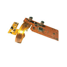
Via-In-Pad: A Game-Changer in PCB Design
Despite its advantages, via in pad technology presents unique challenges during manufacturing. One of the primary concerns is solder wicking, where solder flows into the via, potentially creating voids or weakening the solder joint. To address this, manufacturers use techniques such as via plugging, filling, or capping. These methods seal the vias, ensuring a smooth and solderable surface while maintaining the integrity of the connection. However, these additional processes can increase the complexity and cost of production.
Another challenge is the precision required to implement via-in-pad designs. The technique demands tighter tolerances and meticulous fabrication processes, making it more resource-intensive than conventional PCB designs. While the initial costs may be higher, the long-term benefits in terms of performance, reliability, and space savings often justify the investment.
As electronic devices continue to evolve, via-in-pad technology is becoming increasingly critical for meeting industry demands. Its ability to support miniaturization, enhance performance, and improve thermal management makes it a preferred choice for cutting-edge applications. Whether in consumer electronics, medical devices, or industrial systems, via-in-pad provides the design flexibility needed to create innovative and reliable solutions.
In conclusion, via-in-pad represents a significant leap forward in PCB design. Its capacity to save space, improve electrical and thermal performance, and support high-density layouts makes it an essential tool for modern electronics. While it requires careful implementation and manufacturing expertise, the benefits it offers ensure its place at the forefront of PCB technology.


Leave a Reply