

HDI Technology Impact RF and Microwave Circuits
A high density interconnect pcb is a type of printed circuit board that utilizes intricate copper and via layers to accommodate more components within a smaller footprint. This technology is important for the development of a wide range of advanced electronic devices, from mobile phones and tablets to automobiles and medical equipment. The benefits of HDI technology extend beyond increased component density to include reduced weight, improved performance and lower manufacturing costs.
A key aspect of high-density interconnect PCB design is the strategic arrangement of layers to minimize interference and signal degradation. This process ensures that signals travel through the circuit board in a clear and direct manner, elevating its functionality and signal integrity. This layer-stacking technique is particularly critical for RF and microwave circuits, as it can help to achieve precise impedance control and a high degree of signal fidelity.
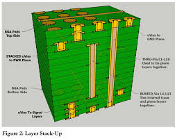
The use of specialized materials and advanced lamination techniques also contribute to the superior electrical properties and functionality of high density interconnect pcb. These materials exhibit exceptional dielectric characteristics that reduce noise and enhance signal timing, helping to elevate the performance of high-density designs. Furthermore, these materials offer superior thermal conductivity, enabling the efficient dissipation of heat generated by densely packed components.
How Does HDI Technology Impact RF and Microwave Circuits?
A core feature of HDI technology is the use of LDI (Laser Direct Imaging) systems for precise imaging during the construction process. Compared to traditional contact imaging, LDI provides much more accuracy and precision for the creation of fine line and spacing features on the PCB substrate. This is crucial for meeting the stringent requirements of modern electronics, where signal clarity and impedance control are essential.
Laser drilling is another key technique that helps to facilitate the production of high-density PCBs. This process enables the production of small-diameter vias, which are essential for achieving higher interconnection densities on HDI circuit boards. This precision is also essential for the creation of complex and fine-pitch features that are necessary for addressing the growing demands of sophisticated electronic devices.
In addition to blind and buried vias, HDI PCBs can also use filled plated microvias to further boost interconnection densities. These are typically larger than blind and buried vias, but still smaller than conventional through-hole vias (PTH). These allow for direct connections between flat lands on different layers of the HDI PCB. As a result, they can help to improve the signal quality on the circuit board while minimizing the number of holes that need to be drilled.
As the world becomes increasingly connected, HDI technology is becoming more commonplace in many areas. For example, smart home and automotive technologies rely on HDI to deliver advanced features that increase efficiency, functionality and security. Additionally, a growing number of industrial applications are using IoT devices to track inventory and monitor equipment performance. This is making them more cost-effective and allowing businesses to save time and money by automating processes. Finally, HDI-enabled medical devices can help to improve the performance and reliability of a variety of electronic products.

)
)
)
)
)
)
)
)
)
)
)
)
)
)
)
)
)
)
)
)
)
)
)
)
)
)
)
)
)
)
)
)
)
)
)
)
)
)
)
)
)
)
)
)
)
)
)
)
)
)
)
)
)
)
)
)
)
)
)
)
)
)
)
)
)
)
)
)
)
)
)
)
)
)
)
)
)
)
)
)
)
)
)
)
)
)
)
)
)
)
)
)
)
)
)
)
)
)
)
)
)
)
)
)
)
)
)
)
)
)
)
)
)
)
)
)
)
)
)
)
)
)
)
)
)
)
)
)
)
)
)
)
)
)
)
)
)
)
)
)
)
)
)
)
)
)
)
)
)
)
)
)
)
)
)
)
)
)
)
)
)
)
)
)
)
)
)
)
)
)
)
)
)
Leave a Reply